Problem
Initially believed to be a problem only with power MOSFETs in a space environment, we now know (2005) that other devices are also susceptible -- including bipolar junction transistors (BJT), insulated gate bipolar transistors (IGBT), thyristors, high voltage diodes, small signal epitaxial npn BJT, and CMOS PWM controllers and drivers. We also now know that these effects extend from outer space down to sea level.
It has been known since 1986 that n-channel power MOSFET transistors (vertical DMOSFETs) biased in the off state can be destroyed by Single Event Burnout (SEB) caused by the heavy ion component of galactic cosmic rays and solar flares found in space environments. It has also been known since 1987 that both n-channel and p-channel power MOSFET transistors can be destroyed by Single Event Gate Rupture (SEGR) in the same environment.
Power MOSFETS are the most susceptible, beginning to show the effect with Vdss voltage ratings in the range of 100 V and higher, although SEB has been reported at less than 30 V bias. BJTs are less susceptible beginning to be susceptible in the range of 400 V or higher. Thyristors and diodes begin to be susceptible in the range of 1,000 V or higher.
At least two mechanisms can lead to destruction in power MOSFETs: Single Event Burnout (SEB) and Single Event Gate Rupture (SEGR), sometimes called Single Event Gate Damage (SEGD). The description below is for n-channel devices.
In SEB an ion that traverses the transistor structure through the source can induce a current flow that turns on the parasitic npn transistor below the source thereby initiating forward biased second breakdown. This leads to device destruction if sufficient short-circuit energy is available.
In SEGD an ion that traverses the transistor through the gate, but avoids the p-regions, can generate a plasma filament through the n-epi layer that applies the drain potential to the gate oxide, damaging (increased gate leakage) or rupturing the gate oxide insulation (device destruction).
Other parts you use in your circuits are also susceptible. Small signal npn epitaxial (as opposed to diffused) BJTs are susceptible to SEB as are CMOS PWM controllers and CMOS driver circuits. Bipolar controllers can experience Single Event Upset (SEU), but not SEB.
SEB and SEGR was first attributed to the heavy ion component of galactic cosmic rays, which are stripped off by the earths atmosphere, but the proton and neutron components also contributed to a much lessor degree. The neutron components can penetrate to sea level and on the way interact with the atmosphere and materials to generate secondary high energy components including high energy protons and recoil ions, such as highly energetic silicon ions. This combination is called terrestrial cosmic rays. These can be significant enough to demand design considerations in avionics equipment. The radiation flux is about 300 times less severe at sea level than it is at 40,000 feet, but can still be the major component to device failure rate at sea level as determined by experiments comparing unshielded failure rate at sea level to failure rates in concrete shielded buildings and in deep salt mines. Also the flux varies with latitude, being 4 times as great at the poles as the equator.
The primary destruction mechanism for SEB in space is a heavy ion passing through the device in its off state generating a plasma filament of electron-hole pairs along its path. In the case of SEB the current caused by the ion path can trigger secondary breakdown (by means of carrier multiplication) in the parasitic transistor in the power MOSFET (or direct secondary breakdown in the case of a BJT transistor.)
In the case of SEGR if the ion path passes through the neck region of a power MOSFET cell, the electrons in the electron hole pair diffuse at a faster rate than the holes and the accumulated holes create a transient field that can exceed the breakdown voltage of the gate oxide causing it to break down. For short breakdown time the device may recover but be degraded by Single Event Gate Damage (SEGD). If longer, a permanent short and SEGR occurs.
A final problem is obtaining data needed for design. First the BVceo of the parasitic transistor is needed for power MOSFET design and the terminals to measure this are not available. In addition, the early test protocols for obtaining the test data use to characterize devices in specification sheets was shown to be inadequate 2003.
Although not destructive, because the energy available to the device is much less, the same mechanisms affect memory and logic circuits and are generally discussed under the terms Single Event Upset (SEU) and Soft Error Rate (SEE).
Relevance
Single event burnout occurs mostly in space where the heavy ion component of cosmic rays and solar flares are the source of the heavy ions. To a lesser extent, terrestrial cosmic rays, that are devoid of heavy ions, can cause the same type problem.
SEB occurs only in power devices at higher voltages where enough energy is available to destroy the device. The voltages of concern is a function of device design. Special circuits techniques or devices designed for radiation environments (RAD HARD) should be considered for voltage of about 28 V or higher.
SEB occurs primarily with n-channel MOSFETS. Experiments show that it is difficult to induce SEB in p-channel devices with normal application derating. SEB is the predominant ion-induced failure mode in non-hardened power MOSFETs.
Both n- and p-channel devices are affected by Single Event Gate Rupture. SEGR failure appears to be the predominant failure mode in hardened power MOSFETs. There could be two reasons for this. First, hardened devices have been designed to minimize SEB and allow application of higher voltages that may enable SEGD. Second, they may have a thinner gate oxide, a technique sometimes used to minimize gate voltage shift with total dose.
Solvability
Power electronic circuits can be designed to operate successfully in radiation environments with acceptable levels of single event burnout and single event gate rupture and other undesired radiation effects. Successful designs result from understanding the environment and selecting and applying parts, including circuit topology and voltage derating, to survive in that environment. The linear energy transfer (LET) spectrum and power MOSFET Single Event Effects (SEE) cross section are useful tools in designing these circuits. Shielding can be considered, but is mostly useless in space and of little use in terrestrial applications.
Shielding
The heavy ion component of cosmic rays in space is so energetic that it is not practical to shield against them in systems such as spacecraft due to shield weight. In terrestrial applications neutrons can be attenuated by shielding. One and a half meters of concrete attenuate the neutrons by an order of magnitude, and three meters attenuate them by two orders of magnitude. This is practical mostly in radiation test environments where many meters of concrete as well as other shielding materials are used.
Environment
The environment is usually specified as an integral LET spectrum that plots the cosmic ray abundance versus LET.
Parts
Both conventional and specially designed radiation hardened power MOSFETs are available. Both have been successfully used in space.
Conventional device usually require a negative gate voltage to hold the device off if total dose is a consideration. The also require a knowledge of the Vceo breakdown voltage (breakdown due to avalanche multiplication) of the power MOSFET parasitic internal transistor, which is never specified in commercial devices and is unavailable for measuremtne due to the base and emitter being shorted and unavailable beneath the surface of the device. Both of these factors complicate a design using non-hardened parts.
The penalty for use of hardened devices is cost. They are much more expensive than their electrical equivalent. These usually solve the SEB and other radiation problems such as total dose, dose rate, and neutron damage, but may still leave a SEGD problem, although it is often minimized. Part data needed for design is the Single Event Effects cross section for the part, which usually has to be measured since it varies between manufacturers for the same part.
Secondary breakdown induced burnout can usually, but not always, be avoided by using power MOSFETS below the BVceo rating of the parasitic bipolar transistor. The safest approach is to use specially designed radiation tolerant or hardened power MOSFETs rated at 200 V or less. These are virtually immune to SEB. The penalty is cost. Radiation hardened power MOSFETs cost much more than their electrical equivalents and they can still be susceptible to SEGR.
Although the needed SEE cross section can be calculated, it is usually measured in simulated cosmic ray environments using the actual part and manufacturer. This data is in non-classified literature and reports and a Jet Propulsion Laboratory (JPL) data base of part test data.
As new power transistor topologies become available, modeling and testing of Single Event Burnout and gate damage of these new parts are necessary to determine part susceptibility to these failure modes.
Application
SEB is a strong function of drain-to-source voltage. This voltage is usually derated to below the BVceo of the MOSFET parasitic npn transistor. This parameter is not usually published and the node necessary to make the measurement is not available in the packaged device. Derating below BVceo used to be considered an absolute cure for SEB, but there is some evidence that SEB can occur with drain to source bias voltages below BVceo
SEB is a function of gate bias with negative gate bias often being used in non-hardened devices to reduce the possibility of SEB.
SEB is also a function of device current.
SEGD is both a function of drain-to-source voltage and gate-to-source voltage.
Temperature affects both, in opposite directions.
Circuit impedance affects the survivability of parts when secondary breakdown occurs. When circuit inductance or resistance limit the available energy sufficiently, SEB failure does not occur. This fact is used in non-destructive test circuits for SEB.
SEGD is usually irreversible, although some annealing of damaged, but not ruptured, oxides has been observed.
Solution
Voltage derating and limiting the energy available to a device are common solution methods. Here solution details are presented as a design procedure to prevent Single Event Burnout. The following solution flow assumes n-channel power MOSFETs.
- Determine radiation environment
- Select circuit topology
- Select part process
- Determine voltage stress
- Select part
- Determine SEE rate
- Redesign if SEE rate is unsatisfactory
Determine Environment
In a non-nuclear-weapon scenario, the space radiation environments of concern are total dose, heavy ions, and protons. Galactic cosmic rays and solar flares contribute to the environment. Since 1980 it has been known that terrestrial cosmic rays can cause the same problem but to a lesser extent. In a nuclear-weapon scenario, neutron fluence, x-ray, prompt gamma, long pulse, multiple events, and electromagnetic pulse are additional concerns. The latter are beyond the scope of this tutorial.
Total Dose
The off characteristics of standard-process n-channel power MOSFET are usually specified at a gate to source voltage of zero volts. As total dose increases, the gate threshold voltage decreases and becomes negative. This can occur at less than 20 k RAD total dose. A negative gate voltage is then necessary to keep the MOSFET off. This complicates the design for no-single-point failure systems. Radiation hardened MOSFETs do not have this characteristic and are held off with zero volts from gate-to-source.
Heavy Ions
The heavy-ion environment is usually specified as an integral LET spectrum. For a given LET on the horizontal axis, the vertical axis gives the number of particles per unit area with an equal or greater LET.
While the impact of the environment on a logic and memory part can be fully characterized by a critical LET derived from the part's Single Event Upset cross section (usually 0.5 of the saturation LET), the same is not true for power MOSFETs.
In power MOSFETs Single Event Effects are a function of drain-source voltage, ion species, energy, range, LET, temperature, and gate bias. Also, the thresholds vary between manufacturers for the same device type. These factors are taken into consideration by varying drain-to-source voltage to obtain the Single Event Effects cross section for the part. Typically there is a drain-to-source threshold voltage for a given gate-to-source bias and LET where failure begins and increases rapidly with voltage. This threshold is determined by a plot of the part SEE cross section versus Vdss.
Cross section for power MOSFETs is usually determined with ions normal to the device surface with LET of 30 MeV/mg/cm2 or greater with a penetration range of 40 microns. The LET is considered satisfactory since the number of particles with LET greater than 30 MeV/mg/cm2 drops off very rapidly on the logarithmic integral LET plot. The range is considered satisfactory since it penetrates through the active area of the device, which 15 to 45 microns depending on BVdss.
Negative gate bias is the worst-case gate bias condition. For SEB, 25 C is worse than higher temperatures (about 10% change from 100 C to 25 C). For SEGD, higher temperature is the worst case. Cross sections vary between manufacturers of the same device type.
Proton
Protons usually do not have sufficient energy to cause SEE directly in power MOSFETs. However, after penetration into a part, they can undergo nuclear reactions with the device silicon nuclei to produce energetic charged particles that can cause SEE. Such particles include alphas, carbon ions, and actual fission of the silicon nucleus. The proton rate can be calculated and added to the galactic cosmic ray rate. Usually the cosmic ray rate predominates.
Select Topology
Vdss Voltage
Most successful power electronics topologies using power MOSFETs in space have been in low voltage (28 V) power systems requiring MOSFETs with BVdss ratings of 100 or 200 volts. In general, the higher the BVdss rating, the more severe the radiation effects on the MOSFET. Given a choice, topologies that require transistors with BVdss of 200 V or less should be used.
Gate Voltage
Gate voltage should never be greater than necessary for operation. Using the gate voltages used to specify turn-on and turn-off time are a good choice.
Impedance
Circuit topologies that externally limit the instantaneous short circuit current through the transistor survive higher LET environments than non-limiting topologies when a device is used at voltages greater than the threshold voltage determined from the cross section.
Duty Cycle
Since SEB occurs only when the MOSFET is off and blocking a voltage selecting a conditions that maximize the on-time to off-time portion of the duty-cycle will reduce the probability of SEB by the same amount. Also, it seems logical that increasing the switching frequency should help since power across the device is removed at a higher rate. This is speculation (on my part) but the experimental evidence indicated higher switching rates improve SEB hardness.
Select Process
Several manufacturers have changed part design and processes to produce a radiation hardened power MOSFET. For example, International Rectifier, in addition to their standard process 100 V 30 A IRF150 part, make a radiation tolerant version and a radiation hardened version. The radiation tolerant IRH7150 is hardened to a total dose of 100 krads and a dose rate of 1 E+11 rads/sec. The radiation hardened IRH8150 is hardened to a total dose of 1 MRad and a dose rate of 1 E+12 rads/sec. Both are characterized at their rated Vdss voltage using Californium with a LET of 40-45 MeV/mg/cm2 and a range of 15 microns and for a copper ion with a LET of 30 MeV/mg/cm2 and range of 40 microns. Test data for other ions, LETs, and range are available in the literature.
The standard process part has been used in total dose environments up to 1 M Rad by biasing the gate-off-voltage negative (typical test data is with positive and negative gate voltages of 10 V) and lot testing.
The penalty for using the radiation tolerant parts is cost. The are much more expensive than their electrical equivalent
Determine Voltage Stress
The voltage stress level is required to determine if a given part will meet requirements in a given environment. The circuit should be analyzed to determine the maximum transient voltage drain to source and the gate OFF voltage when this occurs. Also of interest is the normal gate ON voltage.
Select Parts
Secondary breakdown induced burnout can be avoided by using power MOSFETS below the BVceo rating of the parasitic bipolar transistor.
For standard process parts, care must be taken in selecting the maximum voltage applied to a device since the BVceo is usually not specified, cannot be measured externally, and must be further derated, since measurements have shown SEB in bipolar transistors can occur below the measured BVceo. A guideline used for parts with BVdss of 100 V and 200 V was to derate to 50%. Later test data on both lower and higher BVdss rated parts indicate some parts destroyed at voltages between 20 and 25% of BVdss. For this reason test data is highly recommended for any standard-process part used at greater than 20% of the BVdss rating.
For rad-hardened process parts it can be assumed that test data is available (Jet Propulsion Laboratory (JPL) used to have a data base of such test data but it appears to now be summarized in a published 1998 compendium available in PDF format). Most of this data shows that no destructive SEE occurs at rated BVdss although there are some exceptions. Test data should guide the application, but a 50% derating of BVdss should be more than adequate for rad-hardened parts.
Determine Rate
The rate of Single Event Effects equals the flux above a critical LET threshold multiplied by the part Single Event Effects cross section at the same LET.
Sample calculation:
The SEE cross section versus Vdss of a 100 V IRF150 power MOSFET exposed to 247 MeV copper ions with a LET of 30 MeV-cm2/mg and a range of 40 microns indicates that the SEE cross section is 1 E-4 cm2 at 70 V. If the integral flux spectrum of galactic cosmic rays indicates 2 particles of LET equal or over 30 MeV-cm2/mg are expected during a three year mission life, then the expected Single Event Effects is: (2 events/cm2)*(1 E-4 cm2) = 2 E-4 events over the mission life.
If this is too high, the Vdss voltage could be reduced, a higher voltage part selected, or a rad-hardened part could be used.
Appendices
Appendices - Linear Energy Transfer (LET) and Single Event Effects (SEE) Cross SectionLinear Energy Transfer (LET)
LET
Linear Energy Transfer (LET) is a measure of the energy loss or stopping power of a material for a given heavy ion. The rate of energy loss, dE/dx, is divided by the density of the material being traversed to get LET. Typical units are (MeV)(cm^2.)/(mg).
LET SPECTRUM
The ion environment in space is often specified in a Heinrich curve or integral LET spectrum that plots the cosmic ray abundance versus LET. The vertical axis is the flux of particles integrated over a period of time (seconds, days, mission length). Typical units would be particles per square centimeter per day. Linear Energy Transfer (LET) is the horizontal axis of the plot. Typical units would be (MeV)(cm^2.)/(mg).
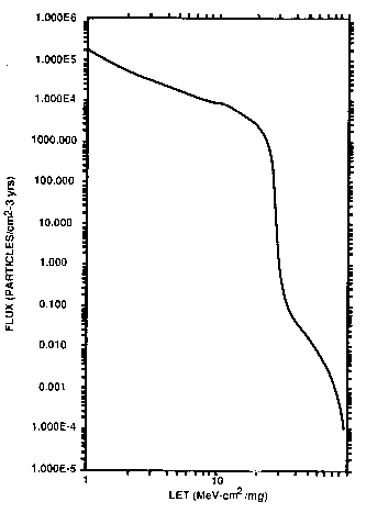
Example Integral Linear Transfer Spectrum
CRITICAL LET
The critical LET is a measure of the onset of Single Event Upset (SEU) in logic and memory circuits. It is measured by rotating a device in an accelerator beam of heavy ions and determining the SEU cross section.
CROSS SECTION
Cross section is defined as the SEB event rate divided by the integral of heavy ion flux (number of events divided by the exposure fluence). As logic and memory devices rotate, the effective LET = LET(0 deg)/cos(theta) increases for device angles not perpendicular to the beam. See Single Event Effects Cross Section for more details.
POWER MOSFETS
In contrast, for power MOSFETs, normal incidence is the worst case and these devices are not rotated. Instead, drain to source voltage is varied. For each voltage, a cross section is determined by dividing the number of events by the exposure fluence. A graph is then made of cross section (cm2) versus applied voltage for a fixed LET.
Single Event Effects (SEE) Cross Section
SEE
Single event effects (error rate, burnout, etc) for a part are determined in experiments using heavy ions in which a uniform beam hits the part.
CROSS SECTION
SEE cross section is defined as the number of upsets observed divided by the number of ions per cm2. The units are cm2.
PLOTS
The SEE cross section is usually plotted as a function of LET.
CRITICAL CHARGE
Critical charge (pC) is the minimum charge deposited in a device's sensitive volume that can cause a Single Effect Event such as changing the state of a logic or memory node.
MOSFETs
For power MOSFETs, a more meaningful plot is cross section versus Vdss, with other parameters such as ion, LET, bias, etc. fixed.
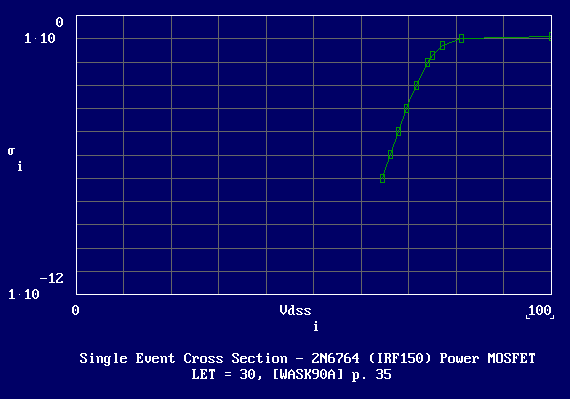
Single Event Cross Section versus Vdss for 2N6764 Power MOSFET
Personal Anecdote
The first time I tested for a radiation event was to test a linear power supply for prompt gamma. The test facility was a linear accelerator at General Atomics in San Diego.
I had studied the somewhat scarce circuit design literature for making circuits radiation hard that was available at the time and applied the principles I had learned.
What a shock when the test results were not what I expected. Weekly modification of the circuit and retesting finally resulted in the desired performance. In fact I got so good at design that when the monitoring scope I used to view the experiments in real time showed unexpected results, I would ask the test engineer to recheck the settings on the official test and monitoring equipment. There was always some calibration error or some other test problem in the "official" test data that was then corrected on the spot.
This was one of the experiences that taught me the value of spending as much time as possible in the lab. The lab is reality, not what you read in text books and application notes. This is one of the things that led to my comment in my lessons learned "I distrust the work of any engineer who spends less than 50% of his/her time in the lab." It would have been impossible to design the circuits if I took the sometimes erroneous test results as being accurate after the opportunity had passed to validate them on the spot and see they were wrong.
I also learned testing can result in radioactive activation of the device and test fixture, which can be a safety hazard. Most electronic materials have short half-life, measured in seconds or hours. However, you might want to avoid materials such as Cobalt, used in some alloys of aluminum and some magnetic cores. Depending on the Colbalt isotope, the half-life may be years. Cobalt 60 has a half-live of 5.3 years. Whatever the material, tested devices are not allowed to leave radio-active storage areas until they are "cool" enough to be released. If you want your breadboard returned in a reasonable time, you may want to pay attention to its construction materials and their half-life.
On the Web
Jet Propulsion Laboratory
The Jet Propulsion Laboratory used to maintain a data base on parts radiation testing accessible by modem. If they still do, I can't find it. However, they do publish a number of papers on the subject including a 1998 compendium of parts data. You can access these papers at their parts resource page. This is a good starting point to see what is available. A good introduction to the impact of radiation in space for electronics, including power devices, are the 139 viewgraphs in Space Radiation Effects on Microelectronics. Papers published by JPL authors from 1997 to 2004 are listed and mostly available in PDF format. Many are on power electronics parts and topics.
IEEE Explore ®
IEEE Explore listed 1,194,402 documents online (August 2005) which resulted in citations for the following search terms related to this page.
- single event burnout -- 46 hits
- single event effects -- 260 hits
- single event upset -- 588 hits
The IEEE is the largest publisher of technical literature in the world and the Explore® database is the premier place to search for it. Anyone can search for citations with abstracts at no cost and pay for articles in PDF form. IEEE members have access to many of the PDF articles at no cost, depending on the Societies they join.
Wikipedia
Wikipedia, the free encyclopedia that anyone can edit, provides explanations for may terms used in this page such as:
- ions : High energy ions are the major cause of SEB and SEGR.
- cosmic ray : Cosmic rays are the source of these ions. Ions are stripped off by the earths atmosphere, therefore ions from space are not a terrestrial problem.
- galactic cosmic ray : The most energetic of these ions are from galactic cosmic rays.
- solar cosmic ray : But solar cosmic rays also contribute ions near earth and sun.
- neutron : The cosmic rays also include neutrons, which can penetrate the atmosphere and interact with material to create secondary ions, protons, and electrons, which can cause terrestrial problems.
- proton : To a lesser extent, protons in space and secondary protons can also be a problem, in both space and terrestrial applications. Secondary radiation can include gamma rays, atomic nuclei, electrons, and alpha particles..
- gamma rays
- atomic nuclei
- electron
- alpha particle Alpha particles can also originate in semiconductor packaging material. This a major problem in single event upset of logic and memory circuits. Surprisingly, this discussed in the Wiki article, although some would argue with the statement that the problem has largely been solved.
Search engines can be used to find other materials on the Internet. For example, Google gives about 529 hits for the phrase "single event burnout" (09/2005). I didn't look at them all, but here are some interesting ones.
- Single Event Effects by Keith E. Holbert, Associate Professor, Arizona State University
- This is an excellent web document on the subject which is of interest to any circuit designer, not just the power supply designer. There is a lot of other related material on Dr. Holbert's website.
References
The papers used to prepare and update this material included on a seperate page, Timeline of Power MOSFET Single Event Burnout Papers with their abstracts and additional notes. The papers have purposely been arranged as a time-line. Reading the abstracts in this time-line order usefully augments what has been discussed on this page.