
The Cole-Hackenberger (Gray) Power Supply

By Arend Lammertink, MScEE. November, 2015.
Introduction
In 1973, Edwin Gray patented a Pulsed Capacitor Discharge Electric Engine, an engine which could produce quite a lot of power seemingly coming out of nowhere. Needless to say, such an engine would change the world, but for various reasons the engine never made it to the market. Over the years, quite a lot of information on these engines has been gathered by Mark McKay, who a/o published an article on the Evolution of the E.V. Gray Circuit Topology in 2004. And even most if not all of the prototypes have resurfaced, although these have been severely damaged in the 1980s. Most of these prototypes have been made by Richard Hackenberger, the technician hired by Edwin Gray to develop this technology, after Marvin Cole, who made the first prototype, left the scene.
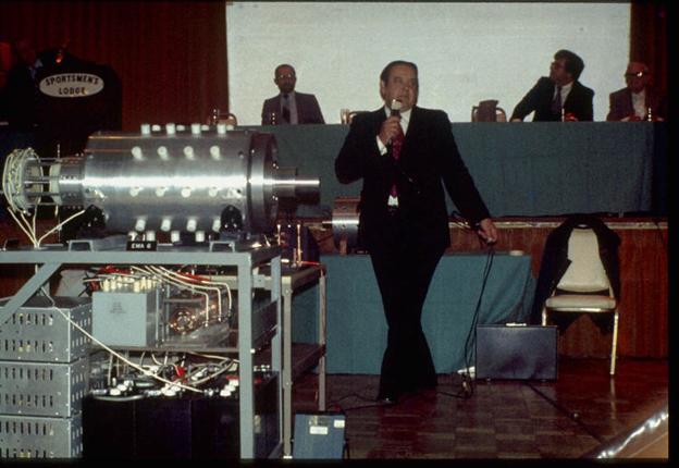
E.V. Gray Version 2.0 type Motor EMA6 1977
Over the years, many people have investigated this technology, which included a/o a rather strange tubes, which were replaced by Ignitrons and/or Thyratrons in later Hackenberger prototypes:.
This strongly suggests that this strange tube must have been a triggered spark gap, or better: triggered arc. Interesting detail is that arcs have a negative resistance area of operation, which can be used to build oscillators, which include radio transmitters. The Poulsen arc radio transmitter, for example, was widely used until the 1920s. If the coils within the engine were indeed part of the tank circuit of a spark gap (arc) oscillator, then it should be no surprise this technology has not been successfully replicated to date.
However, Mark McKay recently brought to my attention that besides these highly complex engine prototypes, Richard Hackenberger also developed a solid state version of the power supply system. Stand alone versions of this power supply have also been demonstrated by Gray, powering an impressive load of over 1 kW, even including a TV-set. In the course of a technical discussion about this with Mark, I came to the conclusion that the power supply unit is essentially a dual solid state Bedini "schoolgirl" oscillator, whereby Hackenberger found an elegant solution to the problem of effectively utilizing the energy John Bedini refers to as "radiant energy", these characteristic BEMF spikes we see in John's systems.
Since Richard Hackenberger and Marvin Cole were the real inventors of this technology, I'd like to refer to this system as the "Cole/Hackenberger Power Supply" (CHPS). Before we discuss the schematics and details of the CHPS, we shall first take a look at the theory and the mechanisms which make this technology possible. At the Energetic Forum, we dubbed this mechanism the "electret effect".
The discovery of the electret effect
My investigation of these kinds of technologies began at the energetic forum, where I joined in 2008. In December 2009, I noted that the similarities between John Bedini's "cold boiling batteries" and Stan Meyer's technology were striking:
Aaron Murakami commented:
Without going into details, we can conclude that there is at least one known practical way to create batteries and electrolytic capacitors which charge themselves for a certain amount of time without any (visible) external power being fed to the system. As a side effect when using batteries, highly explosive hydrogen gas is released, which is called "cold boiling", which introduces hazardous situations. Fortunately, the electrolytes used in electrolytic capacitors prevent hydrogen gas to be released, so these are much safer to work with. You really don't want to be near an exploding (lead acid) battery.
Contrary to most other types of capacitors, the dielectric material which is responsible for most of a capacitors capacity in an electrolytic capacitor does not fill up all the space between the metal plates of the capacitor. Electrolytic capacitors are made by growing a very thin layer of a dielectric material, a material that can be polarized, on one of the metal capacitor plates. The other "plate" is formed by ions in the electrolyte, which fills up most of the space between the metal plates. The other metal plate is merely a contact plate.
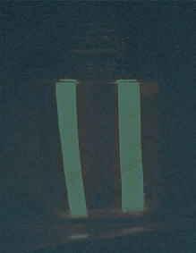
One can actually make electrolytic capacitors quite easily at home and do some experiments, using the recipe of Nyle Steiner. One can also make electrolytic rectifiers, as radio amateurs did in the old days, which are very similar to home made electrolytic capacitors. What is very interesting is that these produce a visible glow during operation:
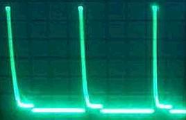
As stated above, it is possible to bring such an electrolytic capacitor into a state that it becomes self-charging, by applying a characteristic "spike" signal to it's terminals. These spikes have a very fast rising edge and a slow falling edge and look like this on an oscilloscope:
In order to understand how this is possible, we first need to know what Porarization of a dielectric material is:
[...]
The interesting detail about the dielectric material within (electrolytic) capacitors is that this polarization is not instantaneous. The (dipole)molecules within a dielectric cannot keep up with a rapidly changing electric field and thus lag behind. This causes the well known Dielectric absorption effect:
[...]
Such a measurement is shown in the following video:
http://www.youtube.com/watch?v=vhHog_yCQ4Q
According to the table on the above page, Aluminium electrolytic capacitors with non-solid electrolyte show the highest absorption, between 10 and 15%. This is important to note, because Aluminum electrolytic capacitors will likely work the best in a CHPS.
On the same page, we find some theory:
Note that the polarization of the dielectric is proportional to the applied electric field and not to the applied current c.q. charge. So, what happens when we momentarily apply a strong electric field to the dielectric so that it polarizes, without actually charging the capacitor by applying a charge current ourselves?
Now wouldn't that be a nice trick to make this Dielectric absorption phenomenon "reload" our capacitor, such that it is the dielectric which charges our capacitor?
Well, that's exactly what can be done by applying these characteristic "Bedini" spikes to an electrolytic capacitor. Peter Lindemann and Aaron Murakami describe this as follows in their Intermediate Bedini SG Handbook:
They also describe that when adding a capacitor charge and discharge (buffer) section to their circuit their battery charges better and faster:
So, while both batteries and electrolytic capacitors can show this "self charging" "electret effect" behavior, this effect is apparently stronger in electrolytic capacitors than in batteries.
However, while this effect has been shown to work in practice, it puts a theoretical problem in front of us: The Law of conservation of energy.
As it turns out, a static electric field can provide energy without breaking the law of conservation of energy. This is explained in detail in the excellent theoretical research of the German Professor Claus Turtur, who also proved his thesis experimentally by showing that the electric field within a high voltage plate capacitor can indeed do work without drawing any current from it's power supply:
http://www.youtube.com/watch?v=IiC2IGLl90Q
In his paper, Prof. Turtur, explains how energy is being converted from Zero-Point Energy into available electric field energy, which can therefore be utilized without breaking the law of conservation of energy.
For a practical analogy, just think of a polarized dielectric material as being kind of a solar panel. A kind of solar panel that does not operate on light (energy) but on zero-point energy. A kind of solar panel that does not provide electric current, but an electric field. An electric field, which can be used to charge an electrolytic capacitor.
In other words: when the right kind of signals are applied to an electrolytic capacitor, it can be thought of as a kind of solar panel which converts zero-point energy into usable electric energy.
So far the basic theory. Let's continue by taking a closer look at John Bedini's technology, who spent years on researching and documenting this phenomenon.
John Bedini's methods
On the website of Panacea-BOCAF, there is a whole page on John Bedini, which includes the following introduction:
His "School Girl" motor is the basic version of his larger multi coil motors, which demonstrates the principle and can easily be built, for example using a wheel from a bicycle. There are a number of magnets attached to the wheel, which come into proximity with a bifilar (transformer) coil, wound around an iron core:

One of the windings is the power winding, the other one is used as a feedback coil, which steers the transistor such that the circuit oscillates once a magnet on the wheel approaches the coil:
This circuit is very similar to an Armstrong oscillator, which also uses a feedback "tickler" coil for steering the transistor or vacuum tube.
When the transistor switches "off", the magnetic field energy built up in the energized coil needs a way out. This causes this characteristic Back EMF (BEMF) to occur, which discharges trough diode D2 to the charging battery.
It is also possible to operate a similar circuit without the wheel, which is called a solid state Schoolgirl (SSSG) circuit, like this one, which also has multiple power coils:
It is also possible to drive the transistor with a separate oscillator, such as a 555 timer circuit, in which case one does not need the feedback coil. In short, there are many ways to create this characteristic "spike" waveform, which all share one important aspect:
The transistor needs to be switched from "on" to "off" as fast as possible.
A lot more information about this can be found in Panacea's overview document, wherein we also find the following note:
Actually, batteries which are charged this way start to behave differently after a while. In fact the chemical substances within the battery appear to change, as has been researched by Dave Rogers:
[...]
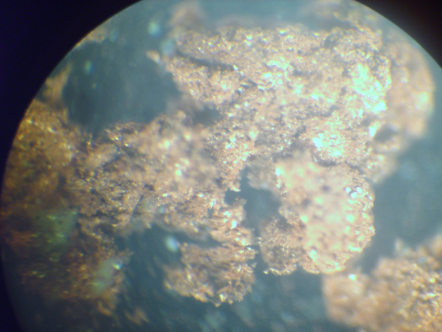
Microscopic close-up of Anode growth. high res
John Bedini and Rick Friedrich also did some experiments with a number of home-made laboratory battery cells:
source: http://www.youtube.com/watch?v=sF5AB7NF51k
Note: this video is no longer available on YouTube. On-site copy here.
Peter Lindemann and Aaron Murakami describe an intriguing detail in their Intermediate Bedini SG Handbook about the nature of the energy of these "spikes":
This observation clearly illustrates that at this point in our analysis the classical lumped circuit model is no longer valid. What we are dealing with, is a transient phenomenon involving impulses, whereby especially the electric field changes so rapidly that longitudinal electric as well as transverse electromagnetic waves, which propagate at the speed of light, are the dominant phenomena which therefore need to be considered.
Contrary to popular belief, both types of waves propagate trough the medium (the aether) itself and do not need free electrons to be present in order to propagate. In most applications, the presence of these waves can be ignored, except when considering (fast) transient phenomena. In the analysis thereof, one needs to fall back to wave propagation models, such as the Telegrapher's equations. And since it appears that the dominant phenomenon to consider is longitudinal waves, we would need to develop an equivalent for the telegrapher's equations for Tesla's single wire transmission system. So, we would need a transmission line model for a single wire transmission line, which I've worked on some time ago.
I'm not too sure my derivation of the longitudinal distributed inductance is correct, but the idea of considering a distributed series resonant LC circuit for describing the longitudinal wave propagating along a single wire transmission line is the correct approach.
Characteristic for this mode of propagation is that there is no return path for the current. There is no current flowing in circles, because this propagation mode embodies the curl-free half of the Helmholtz decomposition which has been totally ignored in Electromagnetic physics:
In a video (probably from the "Energy from the Vacuum" series) John Bedini demonstrates that a neon bulb lights up, when he holds one of it's terminals in his hand and with the other he touches the plastic surface of a battery being charged from his big multi-coil motor. If anything, that makes clear that we are dealing with a situation whereby the classic lumped circuit model is no longer valid and that a strong electric field is present, because the ionization of the gas in a gas-discharge bulb occurs by the presence of a strong electric field.
So, we are looking at a transient electric phenomenon, whereby the BEMF spike we see on the scope has such a steep rising edge that a longitudinal shockwave of possibly enormous magnitude is propagating from the coil to a/o the capacitor and/or battery being "charged", whereby the wires and components from the coil to the capacitor act as a single wire transmission line, whereby the longitudinal shockwave goes trough just about anything, especially any (parasitic) capacitance. However, it does appear to be guided by conductors and probably semiconductors, closed spark gaps (ignitrons), vacuum tubes (thyratrons), etc.
While all of the above does not give us a complete mathematical model of the phenomena at hand, it does give us a rather solid practical foundation which we can build upon. The main problem with Bedini's technology is that John thus far has been unable to "close the loop". However, the power supply c.q. inverter unit developed by Marvin Cole and Richard Hackenberger as part of the EV Gray engine appears to offer a solution to that problem, so let's check it out.
From Bedini to the CHPS
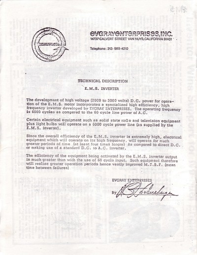
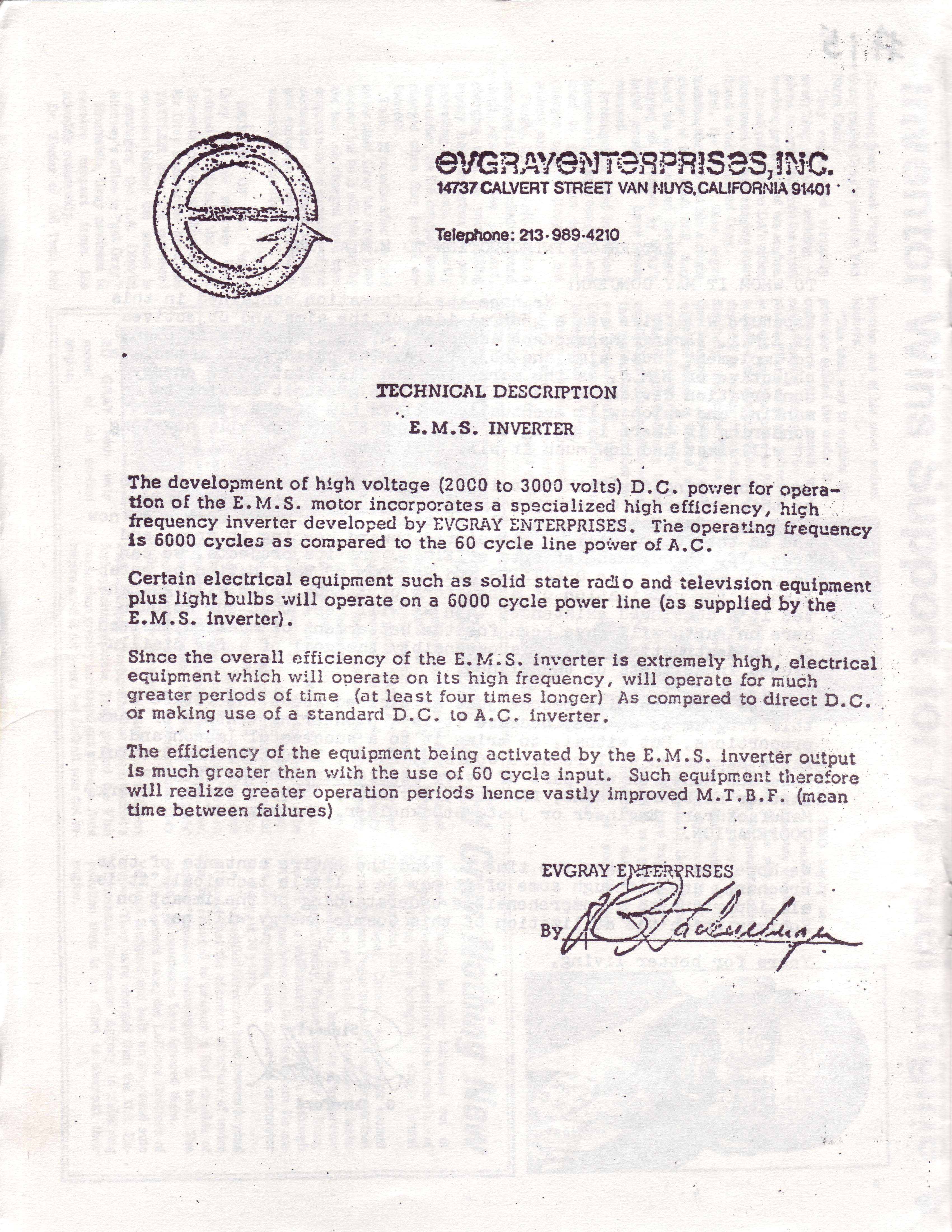
EV Gray and his associates are mostly known for the development of their engine and many researchers have attempted to find out how they managed to realize a COP of no less than 282. A part of this engine was it's power supply, which Hackenberger called the "E.M.S. Inverter" and which was claimed to have a COP of 4:
The text reads:
TECHNICAL DESCRIPTION
E.M.S. INVERTER
According to Mark McKay, Hackenberger said a/o the following things about this "box":
- This little box (here) is what makes that motor go!
- The transformer is the heart of the Generator ---- it will cost 20% more than a regular transformer, but any fabricator can build it. (From Audio Tapes recovered in 2009 & 2014)
- We are feeding it [the load] Chopped DC, and the lower end of the sine wave is going back into the battery again.
- One of the secrets is the transformer; it is the only none off-the-shelf component in the whole system.
- It is not a full sine wave --- If you look at a scope it looks like a hay field. High frequency, high amplitude, very narrow spike.
Some features reported by Mark of this 1979 inverter:
- Substantial Snubber Network
- Negative Bias drive for switching transistors
- Fast fall time for transistors <25 ns
- Transformer has 3 Primary Taps and 4 Secondary Taps
From Hackenberger's "technical description", we learn that the CHPS operated at a frequency of 6 kHz. While at first glance the description might suggest they are able to run "certain electrical equipment" at high voltages, this is not what is actually being said. But it is clear that an inverter existed, which could be used standalone and which was a solid state device. Possibly the 4 secondary taps could be used to produce several voltages, including about 125, as observed by George Dunford, as reported in Mark's 2014 presentation "The Real History of the Ed Gray Motor", showing:
- a 50% duty cycle square wave
- operating at 6 kHz 125 Volts p-p.
In 2010, one of the last inverters ever built (in 1979) was recovered:
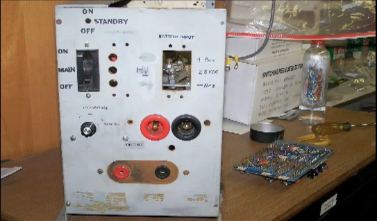
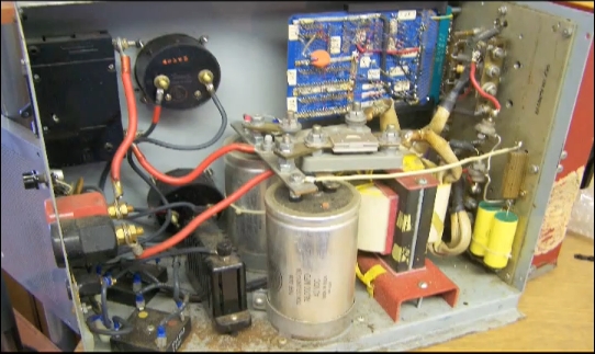
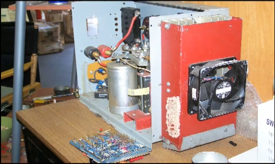
Needless to say, this is an intriguing box, which fascinated Mark. During our e-mail discussion, he mentioned the strange transformer with multiple primaries, which made me remember Matt Jones' paper on the Tesla Switch, which also includes a transformer with two primaries:
Perhaps the first "Tesla Switch" in the public domain has been built by John Bedini, who did not use a dual primary transformer, but he got his "Cigar-Box Size Tesla Switch" working to be demonstrated at the Tesla Centennial Symposium in Colorado Springs, CO, on August, 11, 1984. I don't remember where I saw or read it, but if memory serves me right John once said that this unit required a lot of tuning, whereby he was looking for those "spikes" to occur on the scope during tuning. So, it is likely that the "Tesla Switch" uses the same principle as described above. Matt Jones also referred to the patents of Carlos Benitez, which can also be found with color enhanced illustrations in Patrick Kelly's Book,Chapter 5. Also, Eric Dollard had a similar device which self-sustained the electrical system his car.
Based on this information, I came to the idea that it might be possible to build an inverter with a Bedini-like driver, as I mailed to Mark:
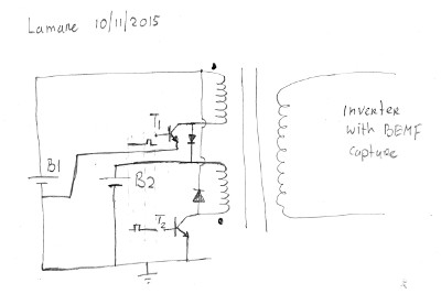
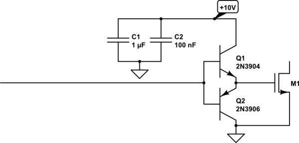
The next day, Mark sent me his schematic from the CHPS, which he painstakingly reconstructed from available photos. It just about blew me away. It was very similar to this sketch, but it included a possible mechanism for "closing the loop" as well as an important detail regarding fast turning off of (bipolar) transistors.
Turning transistors off as fast as possible
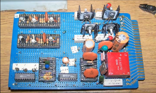
In his 2014 presentation "The Real History of the Ed Gray Motor", Mark included his analysis of the control board of the 1979 CHPS unit:
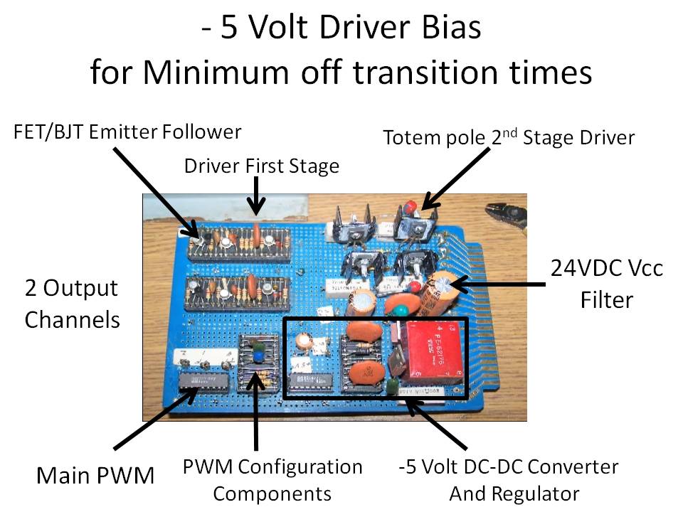
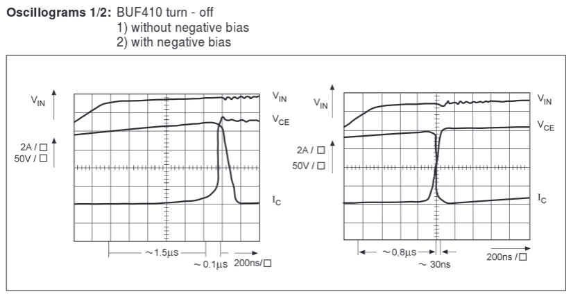
It's not so much the Totem-pole push�pull driver which got my attention, nor the PWM or the first stage driver. It was the -5V DC-DC converter, which was used to provide a -5V bias to the switching transistors in order to minimize the transistor's turn-off times, which is very important to create as strong a BEMF spike as possible. And in order to discharge the base of the transistor as fast as possible, it also makes sense to use a push-pull driver to drive the power transistor.
This technique is not very common, but it is being used in the industry, for example for Fast switch-off of high voltage 4H-SiC npn bipolar junction transistor from deep saturation regime
Quite a lot more information can be found in an STMicroelectronics application note Influence of Gate and Base drive on Power Switch Behaviour:
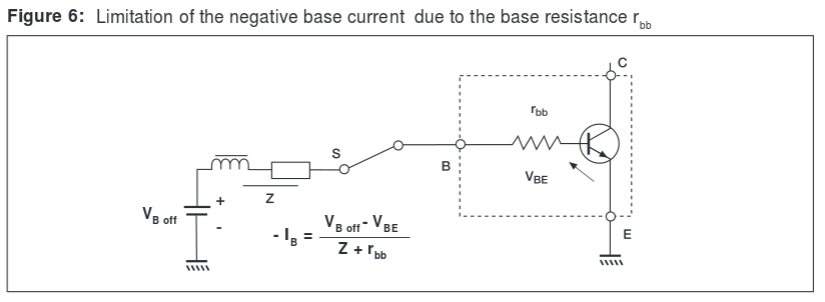
Also some info can be found in Drix' Bipolar FAQ:
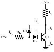
A way to avoid driving a BJT transistor deep into saturation is to use a Baker clamp circuit:
For MOSFET's, there are similar techniques on how to reduce MOSFET turn-off delay:
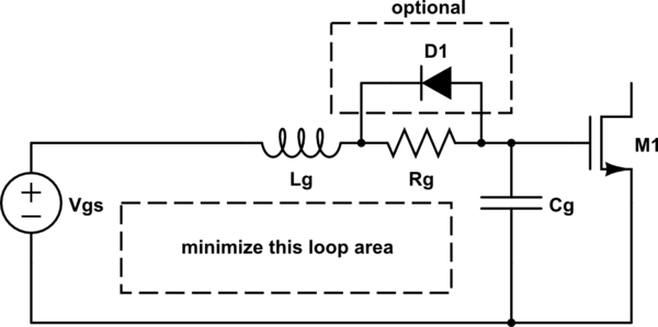
Power semiconductor manufacturer Ixys published an application note "Driving MOSFETs and IGBTs into the 21st Century" (pdf):
One of the techniques they describe is the use of negative bias, illustrated in these figures:

These techniques can also be used for IGBTs or Insulated Gate Bipolar Transistors which have some very interesting properties:
Since Hackenberger employed both thyratrons and triggered spark gaps (Ignitrons), albeit in his engine, and since IGBTs have an excellent ruggedness, the use of IGBTs should definitely be considered for our application. And of course all the above techniques should also be considered in the design of Bedini SG circuits as well as Tesla Switch circuits, because it is very likely that it is these spikes which make it possible to use an electrolytic capacitor or a battery to extract energy out of the vacuum, energy which comes for free.
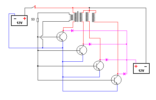
The bowels of the CHPS
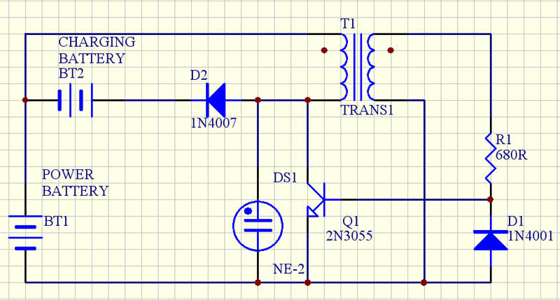
After all the above background information, it is finally time to reveal the schematic of the "Blue Engine Power Supply" from 1979 as far as Mark has been able to reconstruct:
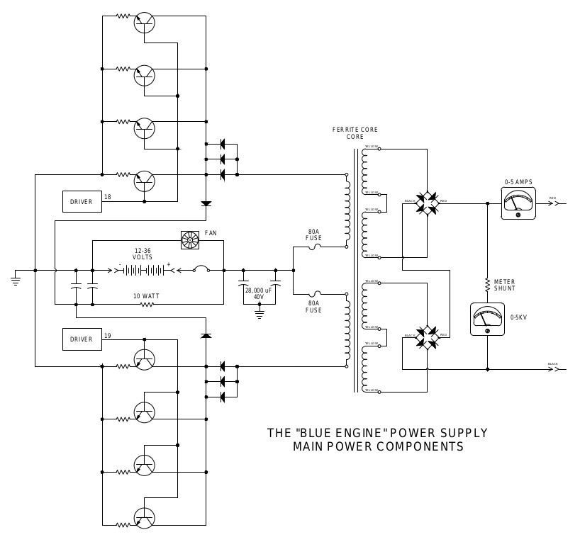
I received this schematic without knowing anything about the CHPS, except that it had two primary windings, just like Matt's Tesla Switch. I immediately recognized the similarity between this schematic and the sketch I made just a day before. I noted that the two BEMF recovery diodes were drawn the wrong way, which I corrected in the above image.
It is also very similar to a basic inverter circuit, which uses the same basic topology as in what Hackenberger called his "E.M.S. inverter":
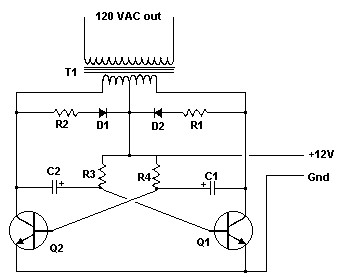
When we compare this basic inverter circuit with a solid state school girl (SSSG) circuit, the CHPS and my sketch above, then we are essentially looking at a dual Bedini SSSG circuit, which is driven back and forth in order to create an alternating magnetic field inside the core, so you can tap A.C. current from the secondary. What basically has to be changed to the basic inverter schematic just above is to remove diodes D1 and D1, which are short-cutting any BEMF spike, and redirect the output of these diode to a circuit which can make use of these BEMF spikes.
In other words: all we really need to do is to apply a twin SSSG circuit to drive this basic inverter circuit, instead of short-cutting the BEMF spikes in the primaries.
While that is the principle, there are quite a lot of details to consider, such as the use of techniques for fast off-switching of the transistor, etc. It should also be noted that the CHPS Mark's schematic is based on has been tampered with and we only have some photographs of it, but I think it should be possible to develop a replication by experimenting with the concepts covered so far.
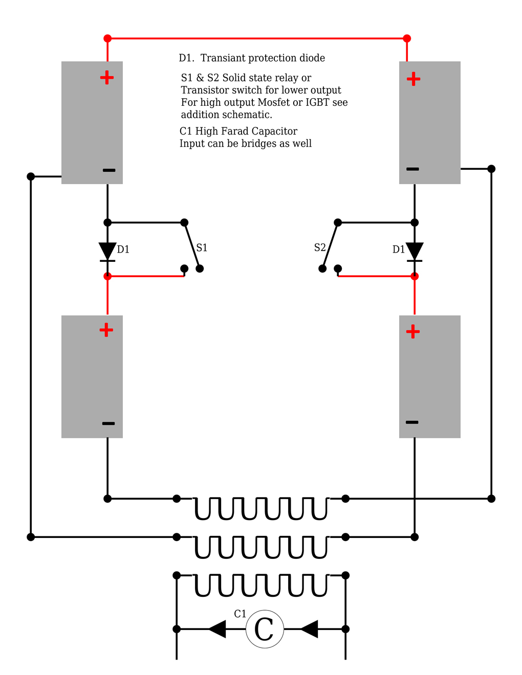
One of the first design choices we will have to make is whether or not to use a tapped primary, or to really split up the two driving sections as much as possible. The CHPS schematic suggests it is possible to use tapped primary, provided you feed the BEMF spike to an (electrolytic) capacitor which is not directly connected to the battery. In the CHPS, there is a 10 Watt resistor of unknown resistance and there also appears to be a third, unused primary in the transformer. Since it would make sense to use a choke coil instead of a resistor, it could be that Hackenberger used that extra primary for that purpose, which may or may not have a positive effect. In the following schematic, I've drawn a tapped primary and a choke coil, which may or may not be on the same core:
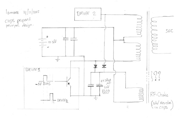
I guess if you were to put it on the same core, you would need some diodes or perhaps a bridge rectifier, which is something I have to take into further consideration. It does seem, though, that the E.M.S. converter started as a system with two batteries and was eventually developed into a system which could do with one battery. In the photo's, I can see only two diodes directly connected to the collectors of the transistors. The other one is isolated and a third may have been moved away from it's original location.